Electron beam welding is a specialist process with a range of advantages for use in the highly sophisticated semi-conductor industry.
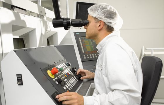
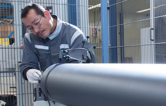
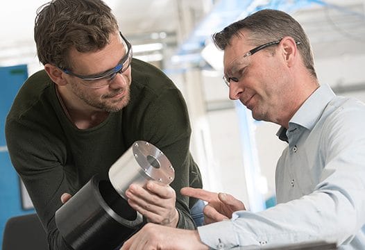
Pronexos has decades of experience in EB welding, with a range of machinery and significant operator experience. We can combine this capability with deep knowledge of the semiconductor industry and significant experience of working with major players and global leaders in the industry.
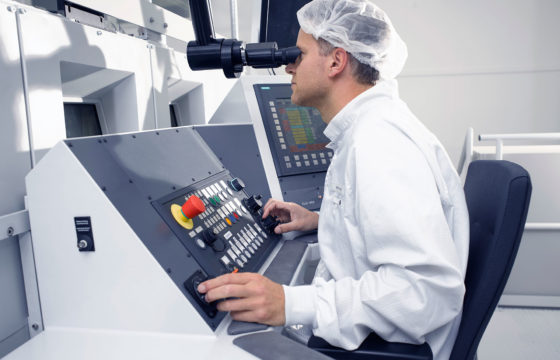
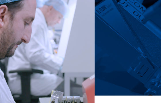
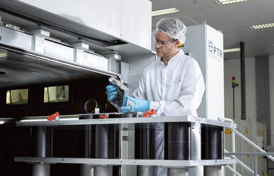
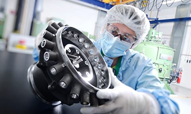
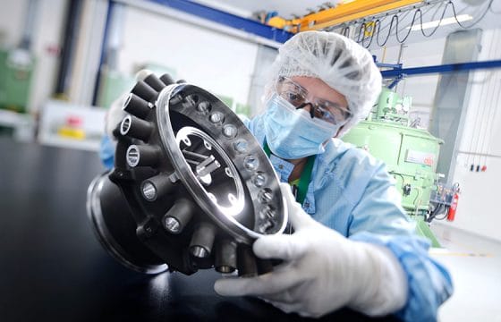
Furthermore at Pronexos we can offer a unique service in being able to deliver EB welding in a clean room environment, a combination which is highly applicable to semiconductors and other micro-electronics.
There are several compelling reasons why EB welding can solve challenges for semiconductor manufacturers:
- Purity – EB welding takes place in a near-perfect vacuum, and for this reason can be used to create high-quality high-precision welds. Welding in a vacuum removes the possibility of contamination in the weld by atmospheric gases that could compromise weld quality
- Precision – Electron beam welding enables very precise welding in areas close to other sensitive materials. The process does not use as much energy as other welding processes and therefore does not create so much heat, so the technique can be used to create very precise welds close to delicate components
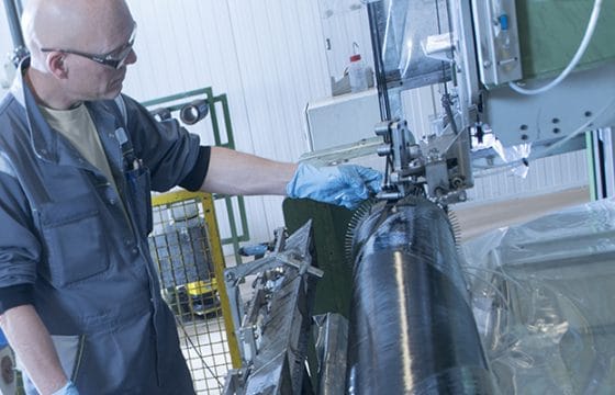
- Range, accuracy and size – EB welding machines in the hands of a skilled and experienced operator can be used to create high quality welds at a great range of sizes, from the width of a human hair to several centimetres thick
- Quality – because EB welding is a very precise process that doesn’t affect the surrounding areas, EB weld processes usually don’t require post-weld work, making it an ideal process for manufacturing delicate semi-conductors and microelectronics. What’s more they are a perfect choice for welds that require post-weld tests such as x-rays or dye tests
- Materials – EB welding enables Pronexos to achieve highly accurate aluminium welds which would not be possible using laser welding techniques. In fact the EB welding process can be used for aluminium, stainless steel and copper, all of which are used regularly in semiconductors.
With its ability to produce stable, repeatable welds to a high degree of accuracy and consistency, EB welding is a great choice for semi-conductor manufacturing processes. In the hands of the right operators, with the right machinery, EB welding can delivery automated high-quality welds, quickly and efficiently, that offers major advantages over other welding processes.